# PCB Design and Manufacturing
## Choosing the Microcontroller
External memory
Internet connectivity
## Terminology
Now that you've got an idea of what a PCB structure is, let's define some terms that you may hear when dealing with PCBs:
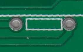
* **Annular ring** - the ring of copper around a plated through hole in a PCB.
[](https://cdn.sparkfun.com/assets/f/0/5/6/e/50d49e1ece395fcf0f000000.jpg) [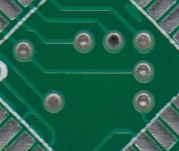](https://cdn.sparkfun.com/assets/d/6/f/2/0/50d49e91ce395fcc0f000002.jpg)
*Examples of annular rings.*
* **DRC** - design rule check. A software check of your design to make sure the design does not contain errors such as traces that incorrectly touch, traces too skinny, or drill holes that are too small.
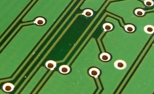
* **Drill hit** - places on a design where a hole should be drilled, or where they actually were drilled on the board. Inaccurate drill hits caused by dull bits are a common manufacturing issue.
[](https://cdn.sparkfun.com/assets/1/d/5/6/8/50d49f0fce395f420c000000.jpg)
*Not so accurate, but functional drill hits.*
* **Finger** - exposed metal pads along the edge of a board, used to create a connection between two circuit boards. Common examples are along the edges of computer expansion or memory boards and older cartridge-based video games.
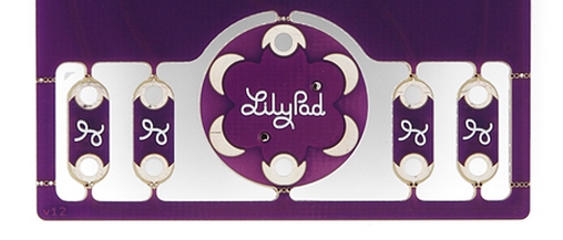
* **Mouse bites** - an alternative to v-score for separating boards from panels. A number of drill hits are clustered close together, creating a weak spot where the board can be broken easily after the fact. See the SparkFun Protosnap boards for a good example.
[](https://cdn.sparkfun.com/assets/7/f/3/8/c/50d4ac6fce395f2b59000000.jpg)
*Mouse bites on the* [*LilyPad ProtoSnap*](https://www.sparkfun.com/products/11201) *allow the PCB to be snapped apart easily.*
* **Pad** - a portion of exposed metal on the surface of a board to which a component is soldered.
[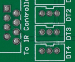](https://cdn.sparkfun.com/assets/c/1/8/b/6/50d4ab81ce395f4c59000002.jpg) [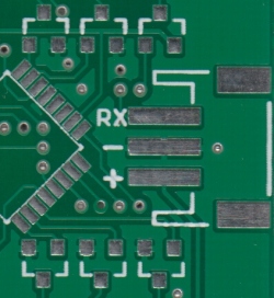](https://cdn.sparkfun.com/assets/8/1/a/b/1/50d4ab81ce395f3959000000.jpg)
*PTH (plated through-hole) pads on the left, SMD (surface mount device) pads on the right.*
* **Panel** - a larger circuit board composed of many smaller boards which will be broken apart before use. Automated circuit board handling equipment frequently has trouble with smaller boards, and by aggregating several boards together at once, the process can be sped up significantly.
* **Paste stencil** - a thin, metal (or sometimes plastic) stencil which lies over the board, allowing solder paste to be deposited in specific areas during assembly.
## Design
In this part, we will discuss the most common mistakes in drawing hardware schematics.
### Looks
Include a description of what your circuit does, what it will be used for. To do that, create a simple block diagram.

Place the wires and pins on the grid. To do that, first make sure that the pin length of the symbols is integer-fold of the grid distance. Otherwise, you might miss an unconnected node. Try to stick with multiples of 100 mil when you create a new schematic symbol. [*Robert Feranec*](https://www.youtube.com/watch?v=lF0UgVQnZ5M) says that people do not want to work on your schematic if you have a mismatch between pin distance and grid distance. 100 mil is a standard grid distance.
Place your components into separate schematic pages according to their functions.
Place the inputs to the left side of the schematic page. Likewise, place the input pins on the left and output pins on the right side of the symbol you create. Power pins look more organized when they are on the top of the symbol. Finally, GND pins would better be placed on the bottom.
Pay close attention to wires carrying important signals such as differential pairs. You need to place net labels to the signals. If they are differential pairs, you need to specify that through "directives". This way these signals will be routed together when you go into PCB part.
Always name all the important nets on the schematic so that you know what is what when you are doing the PCB layout.
### Electrical Concerns
Connections should be done with care following the suggestions on the datasheet of the chip. We are better off with consulting to the following when we draw the schematic of a circuit:
* Datasheet
* Evaluation board
* Starter kit
* Reference schematic
Evaluation board and starter kit give us a hint about whether we may want to consider not using the chip in our schematic. Mostly, if a chip does not have those, there is a risk of missing the important component placements such as a decoupling capacitor when drawing the schematic. Evaluation boards tell us the existence of a working board using the chip involved.
Connect all the input pins on a chip to something unless they have internal pull-up or pull-down. Do not leave them unconnected.
Be careful not to connect critical pins such as output enables to ground or Vcc directly because you may want to try different configurations when you are evaluating your board. Traces to ground and power are very short and hence, difficult to cut physically. Connect them through a resistor for convenience.
Some pins are advised in the datasheet to be connected with coupling capacitors. If there is no information about the capacitance, 100 nF is usually preferred for this purpose.
**Some pins have internal pull-up or pull-down capacitors. This can dramatically affect the voltage on that pin. Be careful while connecting them. It is best to go through all the pins on the chip when making the connections.**
Some pins are specified as open-drain. This means that they are not connected to Vcc on the drain side. With these pins, we specifically need to use external pull up resistors connecting to the correct (specified on datasheets) voltage. [If the pin is going to be used for I2C communication, resistor value is typically chosen as 2K. If it is for GPIO, resistor is 10K.](https://www.robotshop.com/community/forum/t/what-is-open-collector-or-open-drain/13162?gclid=CjwKCAjwyqTqBRAyEiwA8K_4O5njsaaEq4AZs2QEqxKEbXNMR3AFPLawBC4ojyAum11Q8lgW-4u-phoCPFMQAvD_BwE)
When dealing with high speed signals connect the routes directly to the component which is going to use the signal. If you divide the route into parts, and do not use some of them they will disturb the quality of the signal.
#### Decoupling Capacitors
[Their job is to suppress high frequency noise in power supply systems.](https://learn.sparkfun.com/tutorials/capacitors/all) They are usually placed close to power pins and their value is 100 nF. Physically, they should be placed around the chip of concern on the PCB.

For power distribution, we might want to use some filters. You can see the 10 uF capacitor on the input side and the [ferrite bead](https://en.wikipedia.org/wiki/Ferrite_bead) for suppressing noise. Some other advantages of using ferrite bead are when you want to measure current it gives you easy access, and when you want to disable a whole chip it can be de-soldered leaving the chip powerless.
Decoupling capacitors would better be connected around the connectors as well. This makes input and output signals through and from your connectors be much cleaner. You can choose bigger capacitance values depending on the application. If your connector should undergo a current of 1A for example, you can choose to connect 100 uF decoupling capacitor to the corresponding pin.
> To follow good engineering practice, always add at least one decoupling capacitor to every IC. Usually 0.1µF is a good choice, or even add some 1µF or 10µF caps. They're a cheap addition, and they help make sure the chip isn't subjected to big dips or spikes in voltage.
{% hint style="warning" %}
When working with capacitors, it's important to design your circuits with capacitors that have a much higher tolerance than the potentially highest voltage spike in your system.
{% endhint %}
#### Differentail Pairs
These signals like to travel closely. For that, use ribbon cables and place an appropriate header on your PCB.
You need to consider the flow of current when dealing with headers. You need to include more than one path for ground. This makes sure you do not introduce unnecessary resistance to the paths and that they can actually withstand the current they carry.

Do not place critical pins (enable pins, reset pins etc.) close to high frequency pins. You do not want them to interfere.
You might want to consider adding special ESD protection chips close to the connectors.
{% hint style="info" %}
It is a good practice on a standard PCB board to make the traces an absolute minimum of 15 mils (0.381mm) per Ampere. Resource: [Texas Instruments](https://www.ti.com/lit/an/snva021c/snva021c.pdf?ts=1594136289014)
It is good practice to use one standard via per 200 mA of current if the trace will need to conduct a significant amount of current from one plane to the other.
{% endhint %}
## Design Boards that Work the First Time!
There are certain steps you should follow to obtain a design that works like a charm. Here is a summary of them:
#### Import Reference Schematics
Most schematics are in pdf format but we need the source files of them. You can contact the manufacturer to send you the Altium or Orcad source file of the schematics. When you use the reference schematic, you are 100% sure that the schematic works. This is a great advantage.
#### Use the Same Pinout/Connections as in the Reference Circuit
One pin can have many features and one feature can be mapped to different pins. So it is best not to mess with the ordering of the pins and features in the reference circuit.
#### Build Simple Test Circuits
This will save you time and money! Divide the circuit into functions and test them in different boards so that you'll know that it will work again when you place it in the main circuit.
#### Add Extra Components into Your Schematic For Testing
Bypass resistors, pull ups & downs, and optional components definitely help with debugging. Use them with the nets that you are not sure will work. People may sometimes need to cut PCB traces because some component does not work. When you include an extra resistor with that component though, all you need to do is desolder that resistor. Brilliant!
0 ohm resistors are a clever choice for bypassing or rerouting circuits. Footprints give you flexibility to check different components during EMC and EMI testing. Place many footprints around a chip for that purpose.
#### Triple Check Your Libraries
Libraries may sometimes include false footprints of the real hardware. That is a huge frustration if you have already manufactured your PCB. That is why you should always check the dimensions of the footprints against the real hardware. So always buy the chip itself before continuing with the mass production.
Robert Feranec says he prints out the footprints on a paper and compares the dimensions with the real hardware.
#### Check the Schematic Over and Over
A mistake in the schematic cost you a lot of time! A lot more than spending 2 weeks just checking the schematics. Check all the nets in the project one by one.
#### Once Placement is Ready, Build a Paper Model
Placing components on a paper is a good way of giving you an early heads-up before you go on with manufacturing.
#### Reuse the Reference Layout
Going step by step is the key to success. If you are unsure if a component will work, just copy the reference layout and use it in your PCB. As you feel you are getting comfortable with drawing layout, you can gradually move to starting from scratch and building your own board.
#### Follow Design Guides
Some manufacturers include a design guide with their chip. If you follow that, you will be surprised to see your design come to life pretty firmly.
#### Simulate
When you are not sure if your design will work because you changed a lot from the reference design or you broke some rules, you need to check the signal quality on nets via simulation. This will help you make sure everything will work as they are supposed to be in the hardware.
## Critical Points to Consider when Designing a PCB Layout
Every problem (cross-talk, EMI, reflections, skin effects, etc.) in a digital circuit occurs during rise time and fall time. If the signal changes very quickly, we need to pay special attention to the circuit carrying the signal.
Signals need time to travel through a trace. Nothing happens instantly! So consider the time it will take for a signal to travel from the output of a gate to the input of another. This has nothing to do with the clock frequency. It is completely electrical.
We need to consider energy instead of voltage and current. Remember, energy travels within the fields (electrical and magnetic). This field is physically located in between the copper that carries (steers) the signal and the plate underneath. What to do to make sure the components interacts with the fields minimally:
* Keep field volume low. The closer the plates are to the copper, the smaller the volume is.
* Make forward and return paths close to each other.
* Use stitching vias when carrying high speed signals from one layer to another. This will contain the energy field in between the via carrying the signal and the stitching via.

A good article on return paths:
{% embed url="" %}
**Never route across a split plane! This will create an antenna effect and spread the energy everywhere.**


#### 5V trace should use a 5V plane as the reference plane; 3V trace should use a 3V plane. They should never mix!
#### A solid ground plane should never be split!
Here is an article about the worst advises on board stack-up:
{% embed url="" %}
We do not need to fill our vias with conductive material unless it carries a lot of DC current. In all other cases, current travels on the surface of the via.
Adding decoupling caps near transition vias is a good idea when working with low frequency chips (microcontrollers) to eliminate EMI problems.
Working with 4 layer PCBs requires extra care. If layer 2 is power and layer 3 is ground plane, you should not make signals change planes. All signals should be on the same layer so that they do not cause field changes when jumping from layer 1 to 4. **Planes for a 4-layer board suck!** They are so far apart and have so little capacitance to form return paths. If you must use 4-layer stack-up, consider these:

Use the stack-up on the right if you have available space to fit all your components. If it is a crowded design, use the one on the left. Having alternating layers of power and ground is a great practice. Rick Hartley says that every single board he designed since 1995 has power or ground pours on the signal layers.

### About Switching Regulator PCB Design and Resistance and Inductance of Copper Traces
Summing up: In switching regulator layout, it is the AC paths that are considered critical, whereas the DC paths are not. That is the only basic rule to be kept in mind, and from which all the others follow. This is also true for any topology. Perform an analysis of the current flow for any topology in the same manner as we did for the Buck, to find the 'difference traces': and these traces are by definition the 'critical' ones for layout.
What is the problem with step current changes anyway? In a resistor for example, this causes no unexpected/unidentifiable problem. The voltage is given by V=IR, and so for a given change of current, the voltage will change proportionally. For example, a 0.5 cm wide Cu trace of thickness 1.4 mil has a resistance of 1milliohm per cm length (at 20 ºC). So it seems that a 1 inch long trace with a current changeover of 1A, would produce a change in voltage of only 2.5 millivolts across the trace, which is insignificant enough to cause the control sections of most ICs to misbehave. But in fact the induced voltage is much larger. The important thing to realize is that traces of copper on a PCB, though barely resistive, are also inductive. Now, the oft-repeated thumb-rule is that ‘every inch of trace length has an inductance of about 20 nH’. Like the trace resistance, that too doesn’t seem much at first sight. But it is this rather minute inductance which is in fact responsible for a great many customer calls in SIMPLE SWITCHER applications!
{% hint style="warning" %}
The oft-repeated thumb-rule is that ‘every inch of trace length has an inductance of about 20 nH’. Source: [TI SIMPLE SWITCHER® PCB Layout Guidelines](https://www.ti.com/lit/an/snva054c/snva054c.pdf?ts=1594136289120)
{% endhint %}
## Components
### Packaging
{% embed url="" %}
### Capacitors
### Ferrite Beads
{% embed url="" %}
## Calculating the Drill Size
Making the minimum possible drill for the through hole components is important for a firm placement. Here is a great guide on how to choose the drill size:
{% embed url="" %}
In summary, we calculate the maximum hole diameter, add 0.25 mm for the hole, add 0.7 mm for the pad.